No products were found matching your selection.
Our Tailored Flexible PCB Solutions
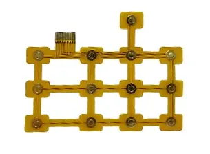
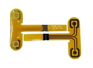
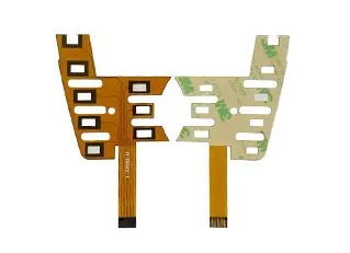
Our flexible PCB customization services offer exceptional bending performance, opening up numerous possibilities in electronics. We produce custom flexible PCBs in various shapes, sizes, and functions. Let us know your requirements, and we'll deliver tailored solutions to meet your specific needs.
At UETPCB, we are committed to quality and innovation. Our advanced manufacturing techniques and rigorous quality control processes ensure that every flexible PCB we produce meets the highest standards of performance and reliability. Whether you need a prototype or high-volume production, our team is ready to support your project with expertise and dedication. Contact us today to discover how our custom flexible PCB services can enhance your electronic designs.
Get a Quote Now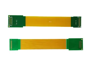
Tailored Flexible PCB Solutions
| Customization Options | Parameter |
|---|---|
| Layers | 1-12 layers |
| PCB Thickness (without stiffener) | 4-40 mil |
| Single Layer Tolerance | ±1.0 mil |
| Double-Layer Tolerance (≤12 mil) | ±1.2 mil |
| Multi-Layer Tolerance (≤12 mil) | ±1.2 mil |
| Multi-Layer Tolerance (12 mil-32 mil) | ±5% |
| Board Thickness Tolerance (including PI stiffener) | ±8% |
| Minimum Board Size | 0.079” x 0.158” (without bridge) 0.315” x 0.315” (with bridge) |
| Maximum Board Size | 8.67” x 27.5” |
| Impedance Control Tolerance | ±5Ω (≤50Ω), ±7% (>50Ω) |
| Minimum Coverlay Bridge | 6 mil |
| Minimum Bend Radius of Single Layer | 3-6 times board thickness |
| Minimum Bend Radius of Double Layer | 7-10 times board thickness |
| Minimum Bend Radius of Multi-Layer | 10-15 times board thickness |
| Minimum Mechanical Drill Hole | 4 mil |
| Inner Layer Trace/Space | 2/2 mil |
| Outer Layer Trace/Space | 2/2 mil |
| Solder Mask Color | Green / Black |
| Surface Treatment | HASL, ENIG, ENEPIG, Electrolytic Nickel Gold, Soft Gold, Hard Gold, Immersion Silver, OSP, Immersion Tin |
| Laser Accuracy (Routing) | ±2 mil |
| Punching Accuracy (Routing) | ±2 mil - ±6 mil |
Customized Flexible PCB Design Solutions

Identify Your Requirements
We discuss your needs and design specifications with you, including circuit layout, size constraints, functionality requirements, and more.

Flexible PCB Design
Utilize specialized design software to create PCB layouts and generate initial design drafts.

Refinement and Revision
We maintain ongoing communication with you to ensure the PCB layout is optimized and meets all requirements.

Prototype Production and Testing
Produce samples for real-world testing and validation to ensure the PCB functions correctly and meets performance standards.

Identify Your Requirements
We discuss your needs and design specifications with you, including circuit layout, size constraints, functionality requirements, and more.

Identify Your Requirements
We discuss your needs and design specifications with you, including circuit layout, size constraints, functionality requirements, and more.
Process of Manufacturing Flexible PCBs
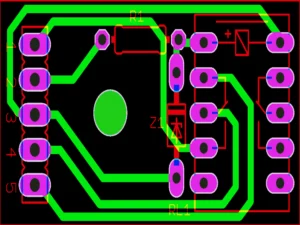
Design and Layout
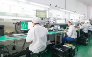
Material Selection

Photolithography
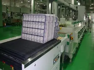
Etching
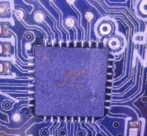
Lamination
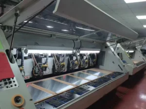
Drilling and Plating
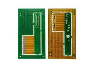
Component Assembly
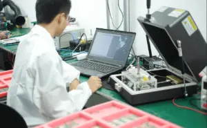
Testing

Finishing
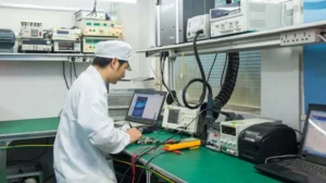
Final Inspection
Benefits of Flexible PCBs
- Flexibility:
Flexible PCBs offer versatility in applications requiring bending, conforming to irregular shapes and curved designs. - Compact Design:
Their slim profile allows for significant space savings in electronic assemblies. - Lightweight Construction:
They contribute to overall weight reduction in products compared to rigid PCBs, making them ideal for lightweight designs. - Enhanced Reliability:
By minimizing interconnection points, flexible PCBs lower failure rates and enhance product reliability. - Cost Efficiency:
Manufacturing costs for flexible PCBs are economical, with simplified assembly processes contributing to cost savings. - Versatile Applications:
Flexible PCBs are well-suited for a wide range of applications, including curved and wearable electronic devices.
FAQs
- What is a Flexible PCB?
A Flexible PCB, or Flexible Printed Circuit Board, is a type of circuit board made from flexible, bendable materials that enable it to conform to various shapes and applications. - What are the advantages of Flexible PCBs?
Flexible PCBs offer benefits such as bendability, space-saving, weight reduction, enhanced reliability, cost efficiency, and versatility in applications like curved and wearable electronics. - What are the typical applications of Flexible PCBs?
Flexible PCBs are used in applications where space-saving, lightweight design, and the ability to bend or conform to irregular shapes are crucial. Examples include smartphones, tablets, medical devices, and automotive electronics. - What materials are used in Flexible PCB manufacturing?
Flexible PCBs are typically made from polyimide or polyester substrates, copper conductors, and protective layers such as solder mask and coverlay. - What are the design considerations for Flexible PCBs?
Design considerations include bend radius, thickness, material selection, impedance control, and the integration of flexible and rigid areas in hybrid designs. - How is the reliability of Flexible PCBs ensured?
Reliable performance is achieved through rigorous testing for mechanical durability, electrical continuity, and adherence to industry standards like IPC-6013. - Can Flexible PCBs withstand harsh environments?
Yes, depending on the materials and coatings used, Flexible PCBs can be designed to withstand harsh environments including high temperatures, moisture, and vibration. - What are the cost considerations when opting for Flexible PCBs?
Costs depend on factors like materials, complexity of design, and manufacturing processes. However, Flexible PCBs can offer cost savings through reduced assembly steps and improved reliability.

